PI: Rafael Jaramillo, Department of Materials Science and Engineering, MIT
Abstract
Photovoltaic (PV) energy converstion is thought to be enhanced by ferroelectricity, but results have been slow due to a lack of materials that combine ferroelectricity at room temperature with absorption of solar light. We will experimentally test a recent theoretical prediction (by a colleague at MIT) of a new ferroelectric semiconductor with band gap in the near-infrared (NIR) and strong visible light absorption. We will make thin film samples and characterize their optical, electronic, and ferroelectric properties, with emphasis on predictors for PV performance. This work will be enabled by a newly-installed molecular beam epitaxy (MBE) system that is designed to enable experimental realizations of theoretically-predicted chalcogenide materials. If successful, this work will have widespread and immediate application in fields beyond PV, including integrated photonics and sensing.
Report
- Project Title: Photo-ferroelectric Materials for Photovoltaics and Photonics
- Principal Investigator: Rafael Jaramillo, Department of Materials Science and Engineering, MIT
- Grant Period: February 2017 – January 2018
Layperson's Description
Semiconductors are materials that can convert light into electricity. The science behind this process has been understood for decades and is the basis for solar cells today. We will explore a new kind of material, called a ferroelectric semiconductor, that may offer a powerful, new mechanism for converting light into electricity. We will test a theoretical prediction of a new ferroelectric semiconductor by making this material for the first time in the laboratory, and measuring its potential for use in solar cells. This project will create new possibilities not just for solar energy, but also for any technology that relies on efficiently converting light into electricity, such as digital imaging.
Project Goals
The goal of this project was to make semiconducting materials that combine ferroelectric polarization with strong light absorption in the visible and near-infrared (NIR). Ferroelectric materials have a built-in electric polarization and produce large voltages when they absorb light, for reasons having to do with the crystal symmetry.1 All known ferroelectric materials have large band gaps and do not absorb visible light. As a result, the large electronic response to light absorption has not been exploited in technology. Research to-date on ferroelectric photovoltaics (PV) has been intriguing but speculative, due in large part to the limitations of the available materials that absorb only a small fraction of the solar spectrum.2–4 For instance, Spanier et al. claim power conversion efficiency beyond the Shockley-Queisser limit in BaTiO3, but the large band gap (Eg ≈ 3 eV) makes the claim difficult to assess.3 In order to develop ferroelectric PV to its full potential we need ferroelectric semiconductors with band gaps in the visible and NIR. To this end, we will experimentally test a theoretical prediction (by a colleague at MIT) of a new ferroelectric semiconductor with band gap in the NIR: Alexie Kolpak (Mechanical Engineering) predicts that ZnSnS3 is a ferroelectric with a band gap of 1.3 eV, which is nearly optimal for PV.5
The specific project tasks were: (1) Grow ZnSnS3 thin films; (2) Characterize material phase and composition; (3) Measure ferroelectric properties through collaboration at MIT. We proposed to make ZnSnS3 thin films by growing epitaxially on GaN (0001), as suggesed by theory,5 using a new molecular beam epitaxy (MBE) system that was delivered to our lab in early 2017. This system was designed specifically to enable the growth of complex, ternary materials containing sulfur and selenium such as ZnSnS3. Due to the mismatch in vapor pressure between ZnS and SnS2, we proposed that ZnSnS3 could be grown by adsorption-limited epitaxy, as was developed decades ago for growing III-V semiconductors.6 This would be an important first demonstration of adsorption-limited growth of complex chalcogenides by MBE.7
Highlights
MBE system installation
The MBE system was installed at MIT in January of 2017. We worked with representatives from the system vendor, Mantis Deposition, to receive delivery of the disassembled system and to install it in the Jaramillo lab. Figure 1 is a picture of the graduate student supported by this Skoltech grant, Stephen Filippone, installing the electron-beam (e-beam) evaporator on the system.
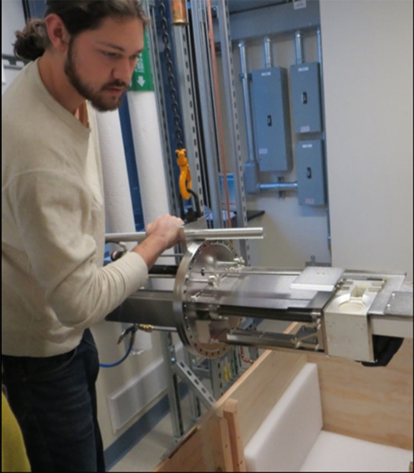
Figure 1: Graduate student Stephen Filippone installing the electron-beam evaporator on the newly-delievered chalcogenide MBE, January 2017.
Theoretical Growth Study
The goals for this project included establishing the adsorption-limited growth technique for a complex sulfide material. The name refers to the condition when the growth rate of a compound material is limited by the arrival and adsorption of one species, independent of the flux of the other species. Adsorption-limited growth is often possible when there exists a large difference in vapor pressure between the two (or more) species being deposited. In such cases, there may exist a window of growth parameters within which the desired solid phase is in thermodynamic equilibrium with the gas phase, with no secondary solid phases present. Adsorption-limited growth was first developed for GaAs, taking advantage of the high vapor pressure of arsenic.6 Adsorption-limited growth is significantly more challenging for complex oxides (such as perovskites), due to the low vapor pressure of most binary oxides, although significant progress has been made with certain materials.8,9
We are not aware of any prior effort to grow ternary chalcogenides by adsorption-limited growth. In order to establish this field, and to assist with our own experiments, we performed thermodynamic simulations of the adsorption-limited growth windows for a number of ternary sulfide and selenide materials ABCh3. We used density functional theory (DFT) to calculate the formation energy of the desired ABCh3 materials, we used the Neumann-Kopp rule to estimate the heat capacity, and we then used FactSage to calculate the equilibrium phase diagram of the A-B-Ch system.10,11 These calculations predict large and easily-accessible windows for adsorption-limited growth of ZnSnS3 for both Zn- and Sn-rich conditions, see Figure 2. This work has recently been published in MRS Communications.12
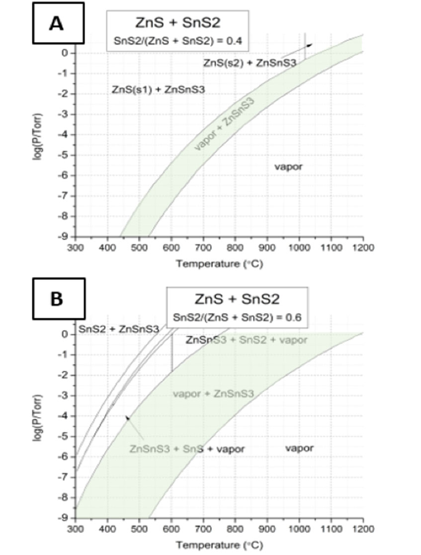
Figure 2: Equilibrium phase diagram for the ZnS-SnS2 quasi-binary system under (A) Zn-rich, and (B) Sn-rich conditions. The horizontal axis indicates the temperature of the growth substrate; the vertical axis indicates the total pressure of all gas-phase species. Adsorption-limited growth windows for ZnSnS3 are colored green, and are easily accessible by our MBE system. Figure from Filippone, Sun & Jaramillo (2018).REF
Next Steps
Film growth
Our efforts to grow ZnSnS3 thin films are ongoing. Our current, main effort is on reducing H2O contamination in the chamber, and the related challenge of maximizing sulfur incorporation in our films. These will be addressed by a new gas delivery system that is currently in-design and will be installed later this year. This upgrade will be funded in part by a separate, ongoing project that requires the same MBE system. When this system is installed we will resume efforts to grow ZnSnS3 epitaxially on GaN (0001), as suggested by theory.5 We will also attempt two-stage growth by depositing Zn-Sn intermetallic films in our MBE, and annealing the GaN / Zn-Sn samples in an H2S environment to make ZnSnS3 by solid-state epitaxy.
Film characterization
We have initiated a collaboration with the Laboratory of Multifunctional Thin Films and Complex Structures at the Institut de Cicncia de Materials de Barcelona (ICMAB), Spain, to characterize the dielectric and ferroelectric properties of our SnZnS3 films. This lab, headed by Prof. Josep Foncuberta, is a world-leader in characterizing ceramic dielectric materials. This collaboration is funded by an MIT-Spain grant, administered by MIT International Science and Technology Initiatives (MISTI) program. The collaboration will include extended visits to ICMAB by the graduate researcher working on this project, Stephen Filippone, with the twin goals of acquiring data on our SnZnS3 films and acquiring relevant knowledge so that the measurement systems and protocols can be established at MIT.
References
1. Fridkin, V. M. Photoferroelectrics. 9, (Springer-Verlag Berlin Heidelberg, 1979).
2. Yuan, Y., Xiao, Z., Yang, B. & Huang, J. Arising applications of ferroelectric materials in photovoltaic devices. J. Mater. Chem. A 2, 6027–6041 (2014).
3. Spanier, J. E., Fridkin, V. M., Rappe, A. M., Akbashev, A. R., Polemi, A., Qi, Y., Gu, Z., Young, S. M., Hawley, C. J., Imbrenda, D., Xiao, G., Bennett-Jackson, A. L. & Johnson, C. L. Power conversion efficiency exceeding the Shockley–Queisser limit in a ferroelectric insulator. Nat. Photonics 10, 611–616 (2016).
4. Zenkevich, A., Matveyev, Y., Maksimova, K., Gaynutdinov, R., Tolstikhina, A. & Fridkin, V. Giant bulk photovoltaic effect in thin ferroelectric BaTiO3 films. Phys. Rev. B 90, 161409 (2014).
5. Kolb, B. & Kolpak, A. M. First-Principles Design and Analysis of an Efficient, Pb-Free Ferroelectric Photovoltaic Absorber Derived from ZnSnO3. Chem. Mater. 27, 5899–5906 (2015).
6. Tsao, J. Y. Materials Fundamentals of Molecular Beam Epitaxy. (Academic Press, 1992).
7. Molecular Beam Epitaxy: From Research to Mass Production. (Elsevier, 2012). at <http://store.elsevier.com/Molecular-Beam-Epitaxy/isbn-9780123878397/>
8. Smith, E. H., Ihlefeld, J. F., Heikes, C. A., Paik, H., Nie, Y., Adamo, C., Heeg, T., Liu, Z.-K. & Schlom, D. G. Exploiting kinetics and thermodynamics to grow phase-pure complex oxides by molecular-beam epitaxy under continuous codeposition. Phys. Rev. Mater. 1, 023403 (2017).
9. Engel-Herbert, R. in Mol. Beam Epitaxy Res. Mass Prod. (ed. Henini, M.) 417–449 (Elsevier, 2012).
10. Leitner, J., Voňka, P., Sedmidubský, D. & Svoboda, P. Application of Neumann–Kopp rule for the estimation of heat capacity of mixed oxides. Thermochim. Acta 497, 7–13 (2010).
11. Bale, C. W., Bélisle, E., Chartrand, P., Decterov, S. A., Eriksson, G., Gheribi, A. E., Hack, K., Jung, I.-H., Kang, Y.-B., Melançon, J., Pelton, A. D., Petersen, S., Robelin, C., Sangster, J., Spencer, P. & Van Ende, M.-A. FactSage thermochemical software and databases, 2010–2016. Calphad 54, 35–53 (2016).
12. Filippone, S. A., Sun, Y.-Y. & Jaramillo, R. Determination of adsorption-controlled growth windows of chalcogenide perovskites. MRS Commun. 8, 145–151 (2018).