PI: Rafael Jaramillo, Department of Materials Science and Engineering, MIT
Abstract
We will develop chalcogenide ferroelectric materials for integrated photonics and solar energy conversion. Theory predicts that certain chalcogenide materials will have ferroelectric polarization and a band gap that is much smaller than traditional oxide ferroelectrics. Such materials could be very space- and energy-efficient at optical modulation, and may feature a giant ferroelectric photovoltaic response to visible or near-IR light. ZnSnS3 is a theoretically predicted ferroelectric material with band gap in the near-IR, at 1.3 eV. We will grow ZnSnS3 thin films by molecular beam epitaxy (MBE), and measure key that are relevant for applications to integrated photonics and photovoltaics. In so-doing we will advance techniques for making epitaxial films of complex chalcogenides by MBE. In a broader sense, this project will contribute to the growth of complex chalcogenides as a new field for electronic materials research, possibly comparable in scope than the field of complex oxides, and yet relatively unexplored.
Report
- Project Title: Chalcogenide Photo-Ferroelectric Semiconductors for Integrated Photonics and Photovoltaics
- Principal Investigator: Rafael Jaramillo, Department of Materials Science and Engineering, MIT
- Grant Period: March 2018 – February 2019
Project Goals
The goal of this project was to make semiconducting materials that combine ferroelectric polarization with strong light absorption in the visible and near-infrared (NIR). Ferroelectric materials have a built-in electric polarization and produce large voltages when they absorb light, for reasons having to do with the crystal symmetry.1 All known ferroelectric materials have large band gaps and do not absorb visible light. As a result, the large electronic response to light absorption has not been exploited in technology. Research to-date on ferroelectric photovoltaics (PV) has been intriguing but speculative, due in large part to the limitations of the available materials that absorb only a small fraction of the solar spectrum.2–4 For instance, Spanier et al. claim power conversion efficiency beyond the Shockley-Queisser limit in BaTiO3, but the large band gap (Eg ≈ 3 eV) makes the claim difficult to assess.3 In order to develop ferroelectric PV to its full potential we need ferroelectric semiconductors with band gaps in the visible and NIR. To this end, we will experimentally test a theoretical prediction of a new ferroelectric semiconductor with band gap in the NIR: Alexie Kolpak (MIT, Mechanical Engineering) predicts that ZnSnS3 is a ferroelectric with a band gap of 1.3 eV, which is nearly optimal for PV.5
The specific project tasks were: (1) Grow ZnSnS3 thin films; (2) Characterize material phase and composition; (3) Measure ferroelectric properties through collaboration at MIT. We proposed to make ZnSnS3 thin films by growing epitaxially on GaN (0001), as suggesed by theory,5 using a new molecular beam epitaxy (MBE) system that was delivered to our lab in early 2017. This system was designed specifically to enable the growth of complex, ternary materials containing sulfur and selenium such as ZnSnS3. Due to the mismatch in vapor pressure between ZnS and SnS2, we proposed that ZnSnS3 could be grown by adsorption-limited epitaxy, as was developed decades ago for growing III-V semiconductors.6 This would be an important first demonstration of adsorption-limited growth of complex chalcogenides by MBE.7
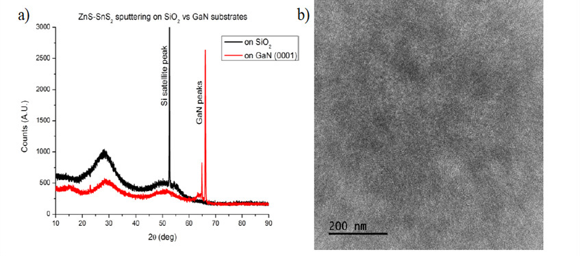
Figure 1: The crystallinity of as deposited co-sputtered ZnS and SnS2 films. a) XRD of films grown on both SiO2 and GaN substrates show broad amorphous x-ray scattering and no well-defined crystallographic planes. b) TEM of amorphous film deposited on SiO2 shows nanocrystalline domains.
Highlights
Film deposition
The growth of ZnSnS3 (ZTS) in MBE started by calibrating the deposition rates from our Sn and ZnS sources. Our Sn is evaporated using an effusion cell. ZnS is deposited using electron beam vapor deposition. Once the rates were calibrated we were able to target the 1:1 metal stoichiometry and co-deposit Sn and ZnS on GaN (0001). Growths were performed in an H2S environment around 10-6 torr.
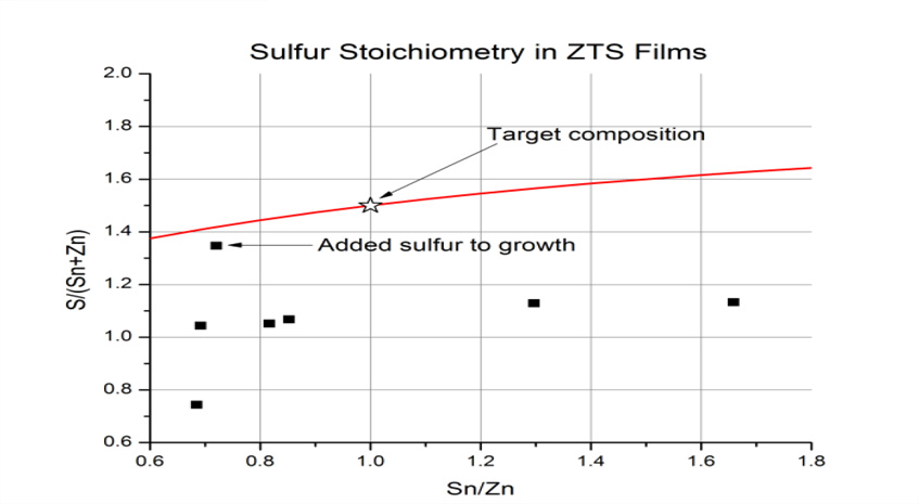
Figure 2: Ratio of sulfur to metal ions as a function of the Sn to Zn ratio. The red lines show the theoretical ratio of sulfur if there was 100% sticking of all sputtered sulfur from the ZnS and SnS2targets. The targeted ZnSnS3 composition is shown by the black star.
Theory specifies that ZTS is stable on a 2x2 surface reconstruction of GaN (0001).5 We followed the cleaning and annealed procedures described in the to get the proper surface reconstruction on GaN.8 Films deposited at a variety of process conditions failed to form ZTS.
Based on success in solid phase epitaxy of Cu2ZnSnS4 and LaCuOS, we decided that this could be an alternative synthesis path for ZTS.9–11 Additionally, reports of sputtering amorphous SnS2 gave added confidence that it would be possible to co-sputter an amorphous ZTS precursor film.12,13 We began as before by calibrating the sputtering rates for our SnS2 and ZnS targets. SnS2 was DC sputtered and ZnS was RF sputtered. Next we cosputtered SnS2 and ZnS films on SiO2 and GaN. We used x-ray diffraction (XRD) to evaluate the film crystallinity (Figure 1). Films were not crystalline but they appeared to have nanocrystalline domains from TEM images. The film composition was measured using wavelength dispersive spectroscopy (WDS).
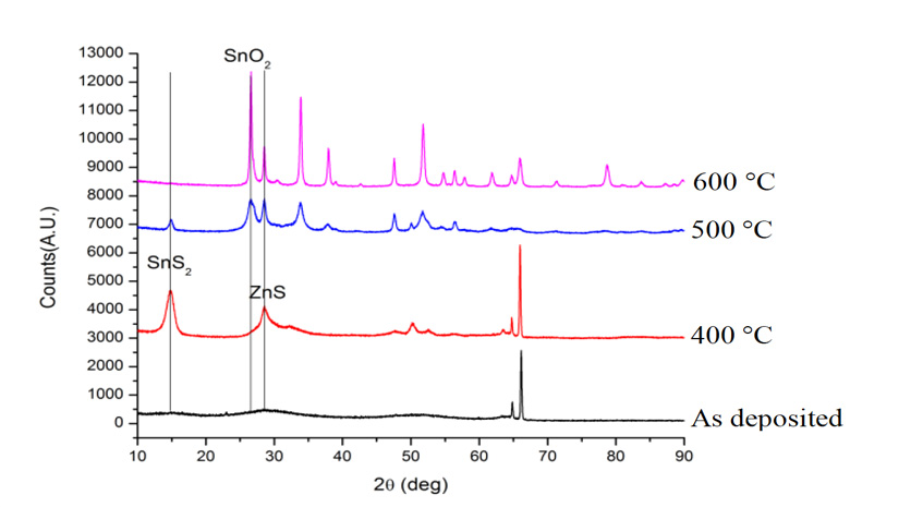
Figure 3: Rapid thermal annealing of cosputtered ZnS and SnS2on GaN (0001). Films were annealed at 400 °C, 500 °C, and 600 °C for 60secin air with N2gas flowing.
We applied a thin film correction to WDS data. We were able to achieve a 1:1 metals ratio but our data shows that are films are very sulfur deficient (Figure 2). The film stoichiometry is approximately SnZnS2. Our next step is to anneal the films for crystallization of the amorphous precursor into crystalline ZTS. An initial annealing attempt in a rapid thermal annealing system that flowed N2 over the sample showed the importance of annealing in oxygen free environments (Figure 3). Above 400 °C, the films formed oxides phases. At 400 °C we got crystallization into ZnS and SnS2 and not ZTS. We are currently optimizing the annealing process.
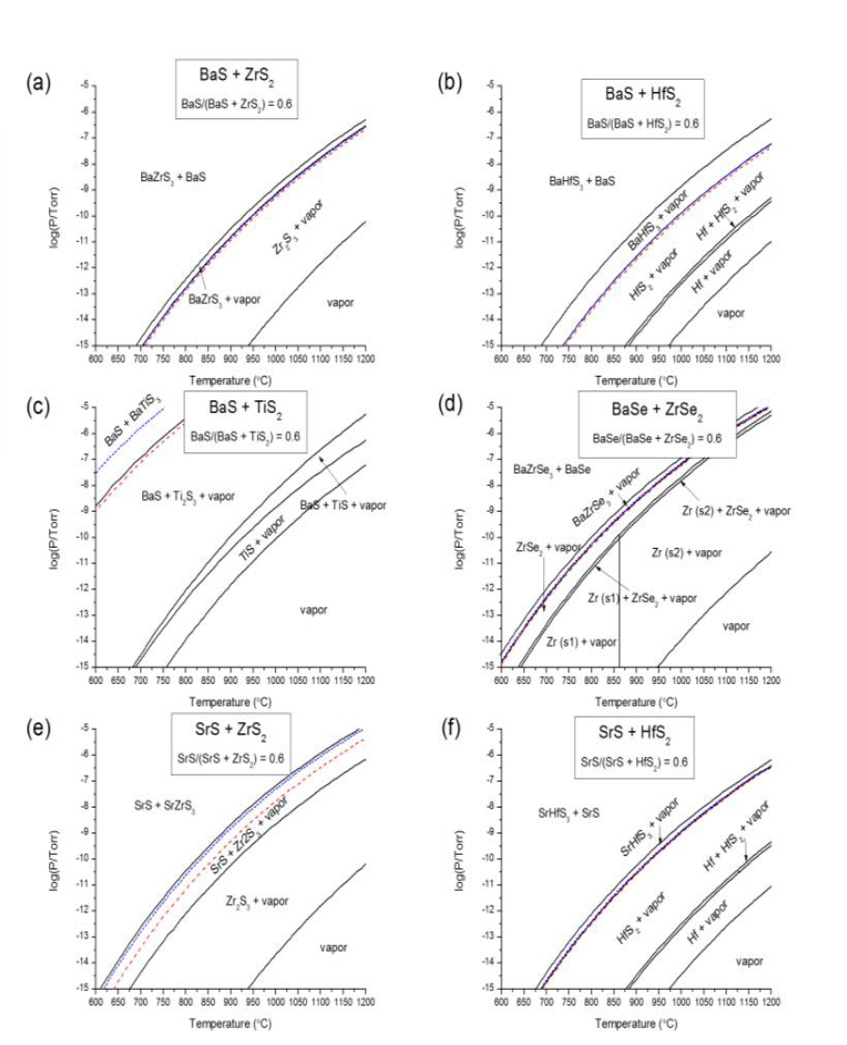
Figure 4: Temperature-pressurephase diagrams for six of the chalcogenide perovskites that are calculated to be thermodynamically stable relative to decomposition into binary chalcogenides. The fixed composition in each case is a mole fraction of 0.6 of the ACh component. The pressure is the sum of the partial pressures of all gas species in the system. In each case, the thermodynamic growth window is labeled “CBCh3 + vapor” for variable elements A, B, and Ch. The calculated enthalpy of formation affects the lower bound of the growth window, if such exists. We show results for calculations using three different functionals, with the corresponding lines indicated by color according to the legend above: PBEsol = green, short dashes; SCAN = blue, longer dashes; SCAN+rVV10 = red, widely-spaced dashes. (a) BaSZrS2 system. (b) BaS-HfS2 system. (c) BaS-TiS2 system. (d) BaSe-ZrSe2 system. (e) SrS-ZrS2 system. (f) SrS-HfS2 system.
Theoretical study
Using improved density functionals, we calculated more accurate formation energies for 18 chalcogenide perovskites and updated our calculated phase diagrams for six target materials (Figure 4). Updated phase diagrams for the other materials is important to the broader goal of developing new materials that interact strongly with light.
Difficulties encountered
In the MBE deposited films, sulfurization of films was our main challenge. In all conditions we tried, we could not get ZTS to form and instead got poorly crystallized ZnS, Sn and SnS2. For these reasons we switched to a solid phase epitaxy (SPE) approach. It may be possible to return to this approach after upgrades to our MBE system which are detailed in a later section.
For sputtered films there are three challenges.
1) Depositing purely amorphous films: XRD experiments indicate that although the films arenot well crystallized, they are neither purely amorphous. Nanocrystalline domains are apparent from TEM images (Figure 1).
2) Sulfur stoichiometry: Sputtered films are sulfur deficient. This is not surprising. Sulfur hasa high vapor pressure and it follows intuition that sulfur may not incorporate into the growing film very well (Figure 2).
3) Annealing: Annealing sulfide materials is a challenge due to their volatility andcorrosiveness. Annealing must occur in oxygen free environments but should also not reduce the sample. Because sulfur contamination is highly undesirable, there are limited resources for annealing. Specifically for ZTS, we are also concerned with secondary phase formation during annealing (Figure 3).
We identified three strategies to address these challenges, as follows.
1) We are experimenting with the sputter process parameters to get more amorphous films.Initial experiments showed an improvement in the amorphous quality of the films whenthey are deposited at a higher rate. Higher rate deposition decreases the diffusion lengthof impinging atoms which tends towards more amorphous film quality. High ratedeposition also has the effect of decreasing the thermal budget of the growth. Since filmsare deposited much faster, they do not get as warm from the sputtering process. Moreexperiments are required to evaluate and understand this. The best strategy to get moreamorphous films is to deposit on a cooled substrate. However, this is currently notpossible in our sputtering system.
2) There are many options for increasing the sulfur content of the films. We could usesulfur-rich targets. A very good way to solve challenges 1 and 2 at the same time is to doion-implantation of sulfur post-deposition. This is actually a very common practice insolid phase epitaxy (DOI: 10.1016/B978-0-444-63304-0.00007-X). A high dose of sulfurion implantation will add sulfur to the film and amorphize any crystalline regions. Wehave already done calculation to determine the dose and implantation energy required forour films. However, sulfur ion implantation is uncommon and therefore, it is anexpensive option. The option we plan to do is to anneal in sulfur environments. This hasto be balanced with other annealing requirements discussed below.
3) To avoid secondary phase formation end encourage epitaxy of ZTS as much as possiblewe will anneal samples in an ultra-high vacuum (UHV) environment. The only downsideto this strategy is that it could further reduce the films. One idea to deal with that is tonucleate ZTS in UHV and then continue crystallization in a sulfur-rich environment.
Currently, we are finishing upgrades to our MBE system that will aide in the completion of this work. Upgrades are focused on improvements to the toxic gas delivery system and adding in-situ characterization capabilities.
Gas-delivery upgrades
Our goal with the upgrades are to remove H2O and O2 from our process gases and to increase the reactivity of hydride gases in our system.
Removal of H2O and O2
We designed and installed a new gas delivery manifold. This manifold has new mass flow controllers that are industry standard in semiconductor processing, meaning the lowest amount of contamination possible. The manifold also features gas purifiers that remove H2O and O2 and other contaminates from our H2S and H2Se gas sources.
Increased H2S reactivity
Based on literature and speaking to experts in gas delivery for growth systems, we have determined that extending the gas delivery tubes in our system should improve the effectiveness of our gas sources. Additionally, we have done calculations that show a 137% increase in the gas pressure at the substrate by extending the gas supply tubes compared to our current gas injection tube positions. We have designed and built an extension that delivers gas as close to the substrate as possible. It is built out of 310SS which is suitable for the high temperature and corrosive environment. Materials with better corrosion resistance at high temperature are difficult to machine and/or not available in small quantities.
Scientific Outlook and Next Steps
The solid phase epitaxy process is divided into two main challenges. First, one must deposit an amorphous precursor film with the correct stoichiometry. We have done that. The second step is to find the correct annealing conditions for epitaxy to occur. Because ZTS is a metastable phase, decomposition into ZnS and SnS2 is a concern during annealing as discussed. To mitigate that risk, we choose to anneal in the adsorption-limited growth conditions we calculated for growth in our MBE (Figure 5). These conditions thermodynamically suppress unwanted secondary phase growth. Annealing in the ultra-high vacuum of our MBE is the next step for this project. Additionally, we will have the option to introduce H2S in our system to tune the sulfur chemistry if needed.
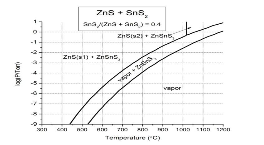
Figure 5: Pressure–temperature equilibrium phase diagrams for the ZnS–SnS2 system. Growth window on Zn-rich side of the phase diagram with SnS2 mole fraction of 0.4.
In this project we have explored two deposition techniques for epitaxy of ZTS on GaN substrates: MBE and SPE. Limitations in our MBE were addressed while we simultaneously pursed the SPE approach. We can soon return to attempting MBE of ZTS. However, the outlook for SPE of ZTS is currently better. We anticipate three main challenges for SPE of ZTS and have discussed multiple approaches for addressing them. Therefore, we plan to finish the SPE growth of ZTS by annealing sputtered films in our MBE.
References
1. Fridkin, V. M. Photoferroelectrics. (Springer-Verlag Berlin Heidelberg, 1979). at<http://www.springer.com/la/book/9783642813535>
2. Yuan, Y., Xiao, Z., Yang, B. & Huang, J. Arising applications of ferroelectric materials inphotovoltaic devices. J. Mater. Chem. A 2, 6027–6041 (2014).
3. Spanier, J. E., Fridkin, V. M., Rappe, A. M., Akbashev, A. R., Polemi, A., Qi, Y., Gu, Z.,Young, S. M., Hawley, C. J., Imbrenda, D., Xiao, G., Bennett-Jackson, A. L. & Johnson, C. L.Power conversion efficiency exceeding the Shockley–Queisser limit in a ferroelectricinsulator. Nat. Photonics 10, 611–616 (2016).
4. Zenkevich, A., Matveyev, Yu., Maksimova, K., Gaynutdinov, R., Tolstikhina, A. & Fridkin,V.Giant bulk photovoltaic effect in thin ferroelectric BaTiO3 films. Phys. Rev. B 90, 161409(2014).
5. Kolb, B. & Kolpak, A. M. First-Principles Design and Analysis of an Efficient, Pb-FreeFerroelectric Photovoltaic Absorber Derived from ZnSnO3. Chem. Mater. 27, 5899–5906(2015).
6. Tsao, J. Y. Materials Fundamentals of Molecular Beam Epitaxy. (Academic Press, 1992).
7. Molecular Beam Epitaxy: From Research to Mass Production. (Elsevier, 2012). at<http://store.elsevier.com/Molecular-Beam-Epitaxy/isbn-9780123878397/>
8. Hattori, A. N., Kawamura, F., Yoshimura, M., Kitaoka, Y., Mori, Y., Hattori, K., Daimon, H.& Endo, K. Chemical etchant dependence of surface structure and morphology on GaN(0001)substrates. Surf. Sci. 604, 1247–1253 (2010).
9. Zhu, Y., Chen, Y., Shen, T., Yi, J., Gan, G. & Huang, Q. Direct current magnetron sputteredCu2ZnSnS4 thin films using a ceramic quaternary target. J. Alloys Compd. 727, 1115–1125(2017).
10. Feng, Y., Lau, T.-K., Cheng, G., Yin, L., Li, Z., Luo, H., Liu, Z., Lu, X., Yang, C. &Xiao, X. A low-temperature formation path toward highly efficient Se-free Cu2ZnSnS4 solar cells fabricated through sputtering and sulfurization. CrystEngComm 18, 1070–1077 (2016).
11. Hiramatsu, H., Ueda, K., Takafuji, K., Ohta, H., Hirano, M., Kamiya, T. & Hosono, H.Fabrication of heteroepitaxial thin films of layered oxychalcogenides LnCuOCh (Ln = La–Nd; Ch = S–Te) by reactive solid-phase epitaxy. J. Mater. Res. 19, 2137–2143 (2004).
12. Banai, R. E., Cordell, J. C., Lindwall, G., Tanen, N. J., Shang, S.-L., Nasr, J. R., Liu, Z.-K., Brownson, J. R. S. & Horn, M. W. Control of Phase in Tin Sulfide Thin Films Produced via RF-Sputtering of SnS2 Target with Post-deposition Annealing. J. Electron. Mater. 45, 499–508 (2016).
13. Sousa, M. G., da Cunha, A. F. & Fernandes, P. A. Annealing of RF-magnetron sputteredSnS2 precursors as a new route for single phase SnS thin films. J. Alloys Compd. 592, 80–85 (2014).